Debrick Huawei HG553 (BCM6358 based router)
Huawei Echolife HG553 is an ADSL2+ modem with WiFi router which was used by some ISP companies in Italy and Spain. The device features a Broadcom BCM6358 dual core processor clocked at 300 MHz with 64 MB RAM.The operating system is stored in a 16 MB flash memory.
The original firmware doesn't offer too many options, but there are alternate firmwares, including OpenWrt which turns this router into a highly configurable network device. If you want to use it for ADSL line, Roleo firmware (D-Link based) is the best choice. For all the other things, OpenWrt remains the best option.
Unlocking and firmware installation procedures are described in various sites. One example is OpenWrt dedicated wiki page for HG553. This post will describe the ultimate debricking procedure: writing bootloader via JTAG. After an unsuccessful firmware update and a forced restart, my router became completely unresponsive. Neither the power LED was on when powered. Reset, Failsafe mode, Telnet for this device didn't exist anymore. In this cases, there is only one solution left: JTAG.
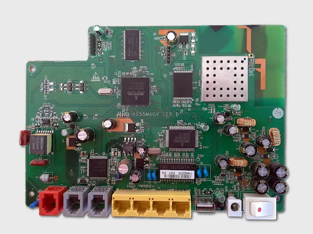
Huawei HG553 main board
JTAG is an interface that allows direct read/write operations on flash memory. Since the router didn't even enter failsafe mode (by holding Reset button and powering up), the most probable cause is a corrupt bootloader. Here is the complete step-by-step guide to debrick this router by rewriting the CFE bootloader. After this procedure you will be able to install compatible firmwares by accessing http://192.168.1.1 after you powered up the router with Reset button pressed.
1. Prepare CFE
CFE (Common Firmware Environment) is the bootloader used by Broadcom chips, including this one. You can get an unlocked CFE from here. Download that archive and you should find acfe.bin file inside. You must open it with a hex editor (I like HxD; can be used in Linux with Wine). The first 256 bytes (from 0x00 to 0xFF) represent a header that doesn't belong in flash memory. It contains some metadata regarding the CFE (size, CRC32). It is not needed, so go ahead and delete the first 256 bytes and save the file.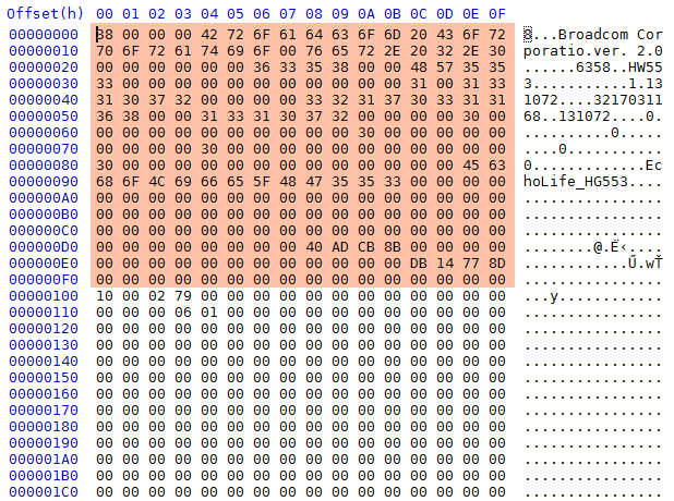
Delete the CFE header
The remaining section must start with 0x10000279. If you find this difficult, get here a headerless CFE, ready for burning to flash. Now you can skip to part 2.Huawei HG553 doesn't care if the bootloader MAC and SN don't match hardware ones. If you want, however, to customize CFE with the MAC address and Serial Number from the back label of your device keep reading here. This information is stored inside NVRAM section. The NVRAM section starts at offset
0x580 (or 0x680 with header). OpenWrt Wiki has a CFE page with more information about this kind of bootloader.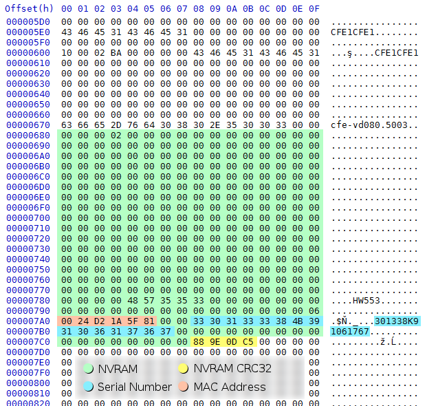
NVRAM MAC address and serial number
Go ahead and edit MAC address (red marked block) in hex mode (on the left column) and serial number on the right column. These are printed on the back label of the router. Edit also the CRC32 (yellow) in hex mode and make it 0x00000000 (put only zeroes in there).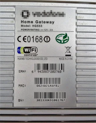
Router MAC and SN on the back label
Click and drag to select that marked block of data (everything in green and yellow, including also bytes you modified) - from 0x580 to 0x6CB (or 0x680 to 0x7CB with header in place), a total of 332 bytes. Save this as a new file. You must calculate CRC32 and put it at offset 0x6C8 (0x7C8).The CRC32 routine is the exact crc32_le() function from Linux kernel. Here is the C source code:
uint32_t crc32_le(uint32_t crc, unsigned char const *p, size_t len)
{
  int i;
        while (len--) {
                crc ^= *p++;
                for (i = 0; i < 8; i++)
                        crc = (crc >> 1) ^ ((crc & 1) ? 0xedb88320 : 0);
        }
        return crc;
}
Download here a small program that calculates CRC32 of a file. You will find there a Windows 32 bit executable and source code for all platforms.Run that program passing as argument the 332 bytes file you created earlier from NVRAM. It will print the CRC32 of that file as, for example:
0x889e0d5. Write your result (i.e. 889E0D5) into the yellow marked block in NVRAM - yes, the one that you zeroed before. Save the CFE file. Now it's ready for burning to flash.2. JTAG Cable
You can use any JTAG adapter you want. The simplest to make is EA253 or DLC5 parallel cable. Below is the schematic and board connection information. The pads for JTAG are on the other side of the board than the one you see in the first image in this post.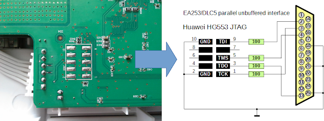
EA253 / DLC5 parallel unbuffered JTAG interface
The cable length should be as short as possible. Connect it to computer and power on the router the usual way.3. JTAG Software
I used with success the free cross-platform UrJTAG software. I could only make it work on Windows though. The procedure is simple:- Set adapter type:
cable EA253 parallel 0x378orcable DLC5 parallel 0x378. - Detect CPU:
detect. - Display system information:
print. - Detect Flash:
detect flash <address>. HG553 uses a Spansion S29GL128N10TF101 chip. - Write flash:
flashmem <offset> cfe.bin.
jtag executable as administrator. Here are all commands:UrJTAG 0.10 #1502
Copyright (C) 2002, 2003 ETC s.r.o.
Copyright (C) 2007, 2008, 2009 Kolja Waschk and the respective authors
UrJTAG is free software, covered by the GNU General Public License, and you are
welcome to change it and/or distribute copies of it under certain conditions.
There is absolutely no warranty for UrJTAG.
WARNING: UrJTAG may damage your hardware!
Type "quit" to exit, "help" for help.
jtag> cable ea253 parallel 0x378
Initializing parallel port at 0x378
jtag> detect
IR length: 5
Chain length: 1
Device Id: 00000110001101011000000101111111 (0x000000000635817F)
Manufacturer: Broadcom
Part(0): BCM6358
Stepping: V1
Filename: c:\program files\urjtag\data/broadcom/bcm6358/bcm6358
ImpCode=00000000100000011000100100000100
EJTAG version: <= 2.0
EJTAG Implementation flags: R4k MIPS16 DMA MIPS32
Clear memory protection bit in DCR
Clear Watchdog
Potential flash base address: [0x0], [0x1f00008c]
Processor successfully switched in debug mode.
jtag> print
(140) String conversion failed!
No.
-----------------------------------------------------------------------------------------------------------------------------------------------------------------
0 Broadcom BCM6358 V1 EJTAG_CONTROL EJCONTROL
Active bus:
*0: EJTAG compatible bus driver via DMA (JTAG part No. 0)
start: 0x00000000, length: 0x1E000000, data width: 32 bit, (USEG : User addresses)
start: 0x1E000000, length: 0x02000000, data width: 16 bit, (FLASH : Addresses in flash (boot=0x1FC000000))
start: 0x20000000, length: 0x60000000, data width: 32 bit, (USEG : User addresses)
start: 0x80000000, length: 0x20000000, data width: 32 bit, (KSEG0: Kernel Unmapped Cached)
start: 0xA0000000, length: 0x20000000, data width: 32 bit, (KSEG1: Kernel Unmapped Uncached)
start: 0xC0000000, length: 0x20000000, data width: 32 bit, (SSEG : Supervisor Mapped)
start: 0xE0000000, length: 0x20000000, data width: 32 bit, (KSEG3: Kernel Mapped)
jtag> detectflash 0x1e000000
Query identification string:
Primary Algorithm Command Set and Control Interface ID Code: 0x0002 (AMD/Fujitsu Standard Command Set)
Alternate Algorithm Command Set and Control Interface ID Code: 0x0000 (null)
Query system interface information:
Vcc Logic Supply Minimum Write/Erase or Write voltage: 2700 mV
Vcc Logic Supply Maximum Write/Erase or Write voltage: 3600 mV
Vpp [Programming] Supply Minimum Write/Erase voltage: 0 mV
Vpp [Programming] Supply Maximum Write/Erase voltage: 0 mV
Typical timeout per single byte/word program: 128 us
Typical timeout for maximum-size multi-byte program: 128 us
Typical timeout per individual block erase: 1024 ms
Typical timeout for full chip erase: 0 ms
Maximum timeout for byte/word program: 1024 us
Maximum timeout for multi-byte program: 4096 us
Maximum timeout per individual block erase: 16384 ms
Maximum timeout for chip erase: 0 ms
Device geometry definition:
Device Size: 16777216 B (16384 KiB, 16 MiB)
Flash Device Interface Code description: 0x0002 (x8/x16)
Maximum number of bytes in multi-byte program: 32
Number of Erase Block Regions within device: 1
Erase Block Region Information:
Region 0:
Erase Block Size: 131072 B (128 KiB)
Number of Erase Blocks: 128
Primary Vendor-Specific Extended Query:
Major version number: 1
Minor version number: 3
Address Sensitive Unlock: Required
Process Technology: Bad value
Erase Suspend: Read/write
Sector Protect: 1 sectors per group
Sector Temporary Unprotect: Supported
Sector Protect/Unprotect Scheme: Bad value
Simultaneous Operation: Not supported
Burst Mode Type: Supported
Page Mode Type: 8 word Page
ACC (Acceleration) Supply Minimum: 11500 mV
ACC (Acceleration) Supply Maximum: 12500 mV
Top/Bottom Sector Flag: Uniform top boot device
Program Suspend: Not supported
jtag> flashmem 0x1e000000 c:\cfe.bin noverify
Chip: AMD Flash
Manufacturer: AMD
Chip: S92GLxxxN
Protected: 0000
program:
flash_unlock_block 0x1E000000 IGNORE
block 0 unlocked
flash_erase_block 0x1E000000
flash_erase_block 0x1E000000 DONE
erasing block 0: 0
addr: 0x1E01FFFE
verify skipped
In the print command output, we can see that flash starts at 0x1E000000. We can use this address to check flash type: detectflash 0x1E000000. Before writing CFE I read some data blocks from flash to see where exactly the CFE is located. And it started directly at flash address. So, launch this command: flashmem 0x1E000000 <cfe.bin_path>. The noverify argument is optional.If flashing fails or doesn't finish (Flash error), check cable, try a shorter one or build a higher quality supported adapter. You could also alter (lower) JTAG clock frequency (
frequency <value>, where value represents frequency in Hz). I got better results with EA253 mode instead of DLC5 using the same cable.After a successful write,
quit UrJTAG and reboot the router. The power LED should be on after a few seconds. You can now access the bootloader and install a firmware.onetransistor.blogspot.com